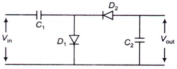
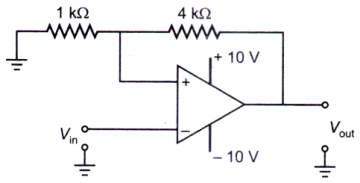
A sinusoidal input voltage V
in of frequency ω is fed to the circuit shown in the figure, where C
1 ≫ C
2 . If V
m is the peak value of the input voltage, then output voltage (V
out ) is
A. 2 V m
B. 2 V o sin ω t
C. D. 2 V m sin ω t
Select an option to see the answer and solution.
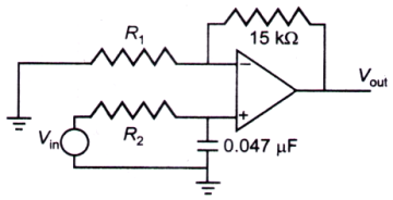
The low-pass active filter shown in the figure has a cut-off frequency of 2 kHz and a pass band gain of 1.5. The values of the resistors are
A. R1 = 10 kΩ 2 = 1.3 Ω
B. R1 = 30 kΩ 2 = 1.3 Ω
C. R1 = 10 kΩ 2 = 1.7 Ω
D. R1 = 30 kΩ 2 = 1.7 Ω
Select an option to see the answer and solution.
The largest analog output voltage from a 6-bit Digital to Analog Converter (DAC) which produces 1.0 V output for a digital input of 010100, is
A. 1.6 V
B. 2.9 V
C. 3.15 V
D. 5.0 V
Select an option to see the answer and solution.
Which one of the sets of values given below does not satisfy the Boolean relation R = PQ' (where, Q' denotes not Q)?
A. P = 1, Q = 1, R = 0
B. P = 1, Q = 1, R = 1
C. P = 0, Q = 0, R = 0
D. P = 0, Q = 1, R = 1
Select an option to see the answer and solution.
In an n-p-n transistor, the leakage current consists of
A. electrons moving from the base to the emitter
B. electrons moving from the collector to the base
C. electrons moving from the collector to the emitter
D. electrons moving from the base to the collector
Select an option to see the answer and solution.
A bipolar junction transistor with one junction forward biased and either the collector or emitter open, operates in the
A. cut-off region
B. saturation region
C. pinch-off region
D. active region
Select an option to see the answer and solution.
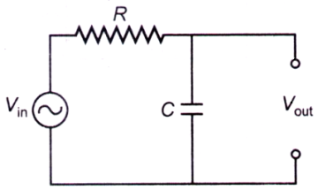
The circuit shown in the figure can be used as a
A. high-pass filter or a differentiator
B. low-pass filter or a differentiator
C. high-pass filter or an integrator
D. low-pass filter or an integrator
Select an option to see the answer and solution.
A field effect transistor is a
A. unipolar device
B. special type of bipolar junction transistor
C. unijunction device
D. device with low input impedance
Select an option to see the answer and solution.
In a typical n-p-n transistor, the doping concentrations in emitter, base and collector regions are CE , CB and CC respectively. These satisfy the relation,
A. CE > CC > CB
B. CE > CB > CC
C. CC > CB > CE
D. CE = CC > CB
Select an option to see the answer and solution.
The simplest logic gate circuit corresponding to the Boolean expression, Y = P + PQ is
Select an option to see the answer and solution.
In one of the following circuits, negative feedback does not operate for a negative input. Which one is it? The op-amps are running from ±15 V supplies.
Select an option to see the answer and solution.
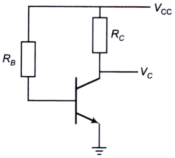
Calculate the collector voltage (V
C ) of the transistor circuit as shown in the figure.
[ Given, α = 0.96, l
CBO = 20 μA, V
BE = 0.3 V, R
B = 100 k
Ω , V
CC = +10 V and R
C = 2.2 k
Ω ]
A. 3.78 V
B. 3.82 V
C. 4.72 V
D. 9.7 V
Select an option to see the answer and solution.
In order to obtain a solution of the differential equation d t 2 d 2 V − 2 d t d V + V 1 = 0 , 1 , an operational amplifier (op-amp) circuit would require at least
A. two op-amp integrators and one op-amp adder
B. two op-amp differentiators and one op-amp adder
C. one op-amp integrator and one op-amp adder
D. one op-amp integrator and one op-amp differentiator and one op-amp adder
Select an option to see the answer and solution.
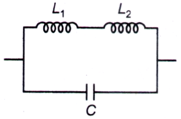
The tank circuit of a Hartley oscillator is shown in the figure. If M is the mutual inductance between the inductors, the oscillation frequency is
Select an option to see the answer and solution.
An avalanche effect is observed in a diode when
A. the forward voltage is less than the breakdown voltage
B. the forward voltage exceeds the breakdown voltage
C. the reverse voltage exceeds the breakdown voltage
D. the diode is heavily doped and forward biased
Select an option to see the answer and solution.
A piece of semiconducting material is introduced into a circuit. If the temperature of the material is raised, the circuit current will
A. increase
B. remain the same
C. decrease
D. cease to flow
Select an option to see the answer and solution.
The voltage resolution of a 12-bit Digital to Analog Converter (DAC), whose output varies from -10 V to +10 V, is approximately
A. 1 mV
B. 5 mV
C. 20 mV
D. 100 mV
Select an option to see the answer and solution.
For an intrinsic semiconductor, m e ∗ m h ∗
A. depends on m e ∗ m h ∗
B. depends on m h ∗ m e ∗
C. depends on both m e ∗ m h ∗
D. depends neither on m e ∗ m h ∗
Select an option to see the answer and solution.
Which of the following statements is correct for a common emitter amplifier circuit?
A. The output is taken from the emitter
B. There is 180° phase shift between input and output voltages
C. There is no phase shift between input and output voltages
D. Both p-n junctions are forward biased
Select an option to see the answer and solution.
Consider the following circuit:
Which of the following correctly represents the output V
out corresponding to the input V
in ?
Select an option to see the answer and solution.