For the junction transistor, which of the following relation is true?
A. α = β − 1 β
B. α = β ( 1 + β )
C. β = 1 − α α
D. β = 1 + α α
Select an option to see the answer and solution.
An op-amp having input voltage Vi1 = 150 µV and Vi2 = 140 µV, differential gain Ad = 4000 and CMRR = 105 . The output voltage of op-amp will be
A. 45.8 mV
B. 45.102 mV
C. 40.006 mV
D. 42.6 mV
Select an option to see the answer and solution.
The load impedance ZL of common emitter amplifier has R and L in series. The phase difference between output and input will be
A. 180°
B. More than 180° but less than 270°
C. 0°
D. More than 90° but less than 180°
Select an option to see the answer and solution.
Match
List-I with
List-II and select the correct answer using the options given below the lists:
List-I (Name of the circuit)List-II (Characteristics of the circuit)
a. Darlington Amplifier
1. A circuit using pnp and npn transistors used in power amplifier.
b. Common base Amplifier
2. A Common-source Amplifier driving a common gate amplifier.
c. Complementary Symmetry Amplifier
3. A Circuit with overall voltage gain close to 1 and very large input impedance.
d. Cascode Amplifier
4. A Circuit with low input impedance mainly used in high frequency applications.
A. a-1, b-2, c-3, d-4
B. a-2, b-1, c-4, d-3
C. a-3, b-4, c-1, d-2
D. a-4, b-3, c-2, d-1
Select an option to see the answer and solution.
The overall bandwidth of two identical voltage amplifiers connected in cascade will be:
A. same as single stage
B. higher than single stage
C. lower than single stage
D. higher if stage gain is low and lower if stage gain is high
Select an option to see the answer and solution.
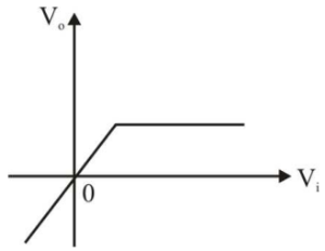
The voltage transfer characteristics as shown in the figure will relate to a
1. Voltage regulator
2. Half-wave rectifier
3. Full-wave rectifier
Which of the above is/are correct?
A. 1 only
B. 2 only
C. 1 and 2
D. 1 and 3
Select an option to see the answer and solution.
A 5 mV, 1 kHz sinusoidal signal is applied to the input of an op-amp integrator for which R = 100 kΩ and C = 1 µF. the output voltage is:
A. 40 π 1 cos ( 2000 π t − 1 )
B. cos ( 2000 π t − 1 )
C. 40 π − 1 cos ( 2000 π t − 1 )
D. − cos ( 2000 π t − 1 )
Select an option to see the answer and solution.
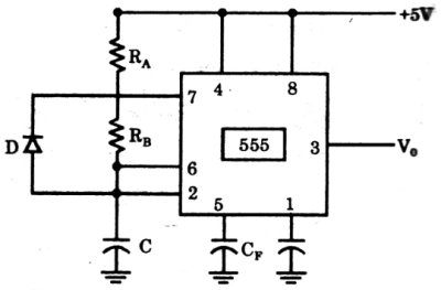
The function of the diode D in the timer circuit shown below is to
A. Increase the charging time of C
B. Decrease the charging time of C
C. Increase the discharging time of C
D. Decrease the discharging time of C
Select an option to see the answer and solution.
An op-amp is used as a zero-crossing detector. If the maximum output voltage is ±15 Volt p-p and the slew rate is 10 V/µsec, then the maximum frequency will be
A. 106 Hz
B. 10.6 Hz
C. 106 kHz
D. 10.6 kHz
Select an option to see the answer and solution.
A voltage VG is applied across a MOS capacitor with metal gate and p-type silicon substrate at T = 300 K. The inversion carrier density (in number of carriers per unit area) for VG = 0.8 V is 2 × 1011 cm-2 . For VG = 1.3 V, the inversion carrier density is 4 × 1011 cm-2 . What is the value of the inversion carrier density for VG = 1.8 V?
A. 4.5 × 1011 cm-2
B. 6.0 × 1011 cm-2
C. 7.2 × 1011 cm-2
D. 8.4 × 1011 cm-2
Select an option to see the answer and solution.
A transistor is said to be useful to be configured as an amplifier when its β is
A. Less than 0
B. Between 0 and 1
C. Between 1 and 50
D. > 50
Select an option to see the answer and solution.
In BJT, DC load line joins
A. IC(more) and VCC
B. IC and VCE
C. IC(Max) and VBE
D. IB and VCE
Select an option to see the answer and solution.
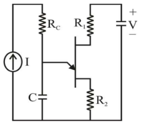
In the circuit of the relaxation oscillator shown in the given figure, what will be the change in the voltage waveform across capacitor, if the voltage V is doubled?
A. The amplitude as well as the frequency of the waveform will get doubled
B. The amplitude will get doubled but the frequency will reduce to half its value
C. The amplitude will get doubled but the frequency will remain unchanged
D. The Amplitude will remain unchanged but the frequency will get double
Select an option to see the answer and solution.
An N-channel JFET, having a pinch-off voltage (Vp ) of -5V, shows a trans conductance (gm ) of 1 mA/V when the applied gate-to-source voltage (VGS ) is -3V. Its maximum trans conductance (in mA/V) is
Select an option to see the answer and solution.
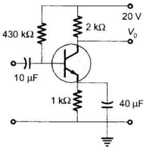
The circuit using a BJT with β = 50 and V
BE = 0.7 V is shown in the figure. The base current I
B and collector voltage V
C are respectively
A. 43 µA and 11.4 volts
B. 40 µA and 16 volts
C. 45 µA and 11 volts
D. 50 µA and 10 volts
Select an option to see the answer and solution.
The use of rectifier filter in a capacitor circuit gives satisfactory performance only when the load
A. current is high
B. current is low
C. voltage is high
D. voltage is low
Select an option to see the answer and solution.
In op-amp based inverting amplifier with a gain of 100 and feedback resistance of 47 kΩ, the op-amp input offset voltage is 6 mV and input bias current is 500 nA. the output offset voltage due to an input offset voltage and an input bias current, are
A. 300 mV and 23.5 mV
B. 606 mV and 47.0 mV
C. 300 mV and 47.0 mV
D. 606 mV and 23.5 mV
Select an option to see the answer and solution.
The Ebers Moll model is applicable to
A. Bipolar junction transistors
B. NMOS transistors
C. Unipolar junction transistors
D. Junction field-effect
Select an option to see the answer and solution.
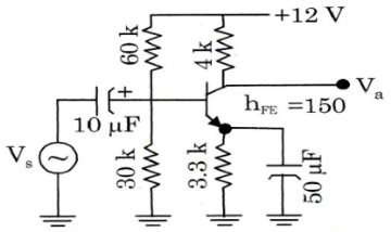
An amplifier circuit is shown in the given figure:
The voltage gain
( V s V 0 ) is:
Select an option to see the answer and solution.
A peak detector comprises a capacitor and an ideal diode and an ac source in series.
A. The instantaneous current depends only on the instantaneous source voltage
B. The diode voltage is always zero
C. The instantaneous current depends only on the diode
D. The energy stored in the capacitor can never decreases with time
Select an option to see the answer and solution.