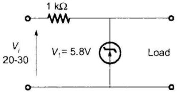
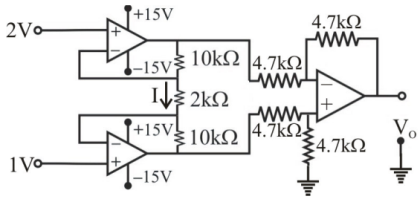
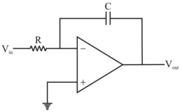
The Zener diode in the regulator circuit shown in the figure has a Zener voltage of 5.8 volts and a Zener knee current of 0.5 mA. The maximum load current drawn from this circuit ensuring proper functioning over the input voltage range between 20 and 30 volts, is
With reference to the negative feedback voltage - series configuration, which of the following statements is/are correct?
1. Bandwidth increases.
2. Non-linear distortion decreases.
Select correct answer.
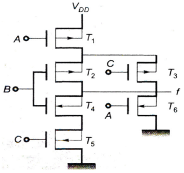
In figure T1, T2 and T3 are p-channel MOS transistors, and T4, T5 and T6 are n-channel MOS transistors. A, B and C are binary signals. The output f(A, B, C) is
For a class-A power amplifier, supply dc voltage is ± 12 V, the quiescent collector current is 72 mA and the load resistance is 100 Ω. If the output voltage across the load is 12 V peak-to-peak, the efficiency of the amplifier is (neglect the loss occurring in the biasing resistors):
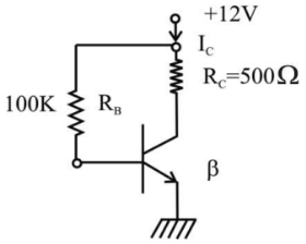
In the base biased transistor circuit, the junction temperature may vary from 25°C to 75°C. If β increase from 100 to 150 with raising temperature, percentage change in VCE point will be
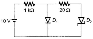
In the figure, assume that the forward voltage drops of the PN diode D1 and Schottky diode D2 are 0.7 V and 0.3 V, respectively. If ON denotes conducting state of the diode and OFF denotes non-conducting state of the diode, then in the circuit,
Biasing is used in transistor amplifiers to
1. Stabilize the operating point against temperature variations.
2. Place the operating point in the linear region of the characteristics.
3. Make α, β and ICO of the transistor independent of temperature variations.
4. Reduce distortion and increases dynamic range.