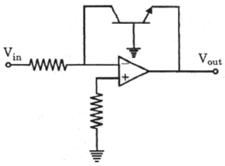
The op-amp circuit shown in the given figure be used for
A. Addition
B. Subtraction
C. Both addition and subtraction
D. Logarithmic
Select an option to see the answer and solution.
Transistors ratings symbols using capital letter and with subscripts also in capital letters denotes
A. DC parameters
B. AC parameters
C. Effective values
D. Time varying values
Select an option to see the answer and solution.
Crest factor for an alternating current source is the ratio of
A. Maximum value of RMS value
B. RMS value to maximum value
C. RMS value to average value
D. Maximum value to average value
Select an option to see the answer and solution.
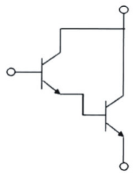
Each Transistor in Darlington pair (as shown in Fig.) has h
fe = 100. Overall h
fe of composite transistor neglecting leakage current is,
A. 10000
B. 10001
C. 10100
D. 10200
Select an option to see the answer and solution.
An amplifier's power level is changed from 8, watts to 16 watts, equivalent dB gain is
Select an option to see the answer and solution.
In common emitter BJT amplifier, the maximum usable supply voltage is limited by
A. Avalanche breakdown of Base-Emitter junction
B. Collector-Base breakdown voltage with emitter open (BVCBO )
C. Collector-Emitter breakdown voltage with base open (BVCBO )
D. Zener breakdown voltage of the Emitter-Base junction
Select an option to see the answer and solution.
Which of the following circuits converts any arbitrary waveform into square waveform?
A. Hartley oscillator
B. Schmitt trigger
C. Differentiator
D. RC phase shift oscillator
Select an option to see the answer and solution.
In a hybrid π model, which terminal is NOT accessible?
A. Emitter
B. Collector
C. Induced base
D. Virtual base
Select an option to see the answer and solution.
Calculate the value of IE for a transistor that has αdc = 0.98 and IB = 100 µA.
A. 5.0 mA
B. 4.8 mA
C. 4.9 mA
D. 6.4 mA
Select an option to see the answer and solution.
For an amplifier, which parameter is calculated with VS = 0?
Select an option to see the answer and solution.
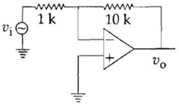
Input resistance of inverting amplifier as shown in figure with ideal op-amp is:
Select an option to see the answer and solution.
In an op-amp, if the feedback voltage is reduced by connecting a voltage divider at the output, which of the following will happen?
A. 1 only
B. 2 only
C. 3 only
D. 1, 2 and 3
Select an option to see the answer and solution.
The reason for using a precision OPAMP based rectifier diode for detecting weak AM signals is that
A. the demodulation is easy
B. the signal is amplified and power is less
C. the noise is less and easy to filter
D. the cut-in voltage of the diode is reduced
Select an option to see the answer and solution.
Negative feedback amplifier is a . . . . . . . .
A. Degenerative feedback
B. Regenerative feedback
C. Both A and B
D. None
Select an option to see the answer and solution.
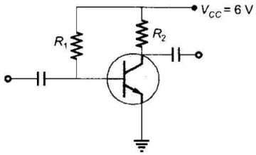
In the amplifier circuit shown in the figure, the values of R
1 and R
2 are such that the transistor is operating at V
CE = 3 V and I
C = 1.5 mA when its β is 150. For a transistor with β of 200, the operating point (V
CE , I
C ) is
A. (2 V, 2 mA)
B. (3 V, 2 mA)
C. (4 V, 2 mA)
D. (4 V, 1 mA)
Select an option to see the answer and solution.
In the break region of clipping circuit, a diode behaves as
A. fully on
B. it is difficult to decide
C. fully off
D. neither fully on nor fully off
Select an option to see the answer and solution.
One of effect of negative feedback in amplifier is to
A. Decrease the harmonic distortion
B. Increase the harmonic distortion
C. Decrease the bandwidth
D. Increase the noise
Select an option to see the answer and solution.
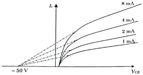
Output characteristics of a BJT amplifier is given. Find the minimum collector current required for r
0 = 50 kΩ. (r
0 is output resistance)
A. 1 mA
B. 5 mA
C. 10 mA
D. 100 mA
Select an option to see the answer and solution.
An N-Channel JFET has IDSS = 8 mA and Vp = -5 V. The minimum value of VDS for pinch-off region and the drain current IDS for a VGS = -2V are.
A. 3 V and 2.88 mA
B. -5 V and 1.88 mA
C. -2V and 3.12 mA
D. -7 V and 1.98 mA
Select an option to see the answer and solution.
From measurement of the rise time of the output pulse of an amplifier whose input is a small amplitude square wave, one can estimate the following parameter of the amplifier.
A. Gain-bandwidth product
B. Upper-3-dB frequency
C. Lower-3-dB frequency
D. Slew-Rate
Select an option to see the answer and solution.