An amplifier using BJT has two identical stages each having a lower cut-off (3 dB) frequency of 64 Hz due to coupling capacitor. The emitter bypass capacitor also provides a lower cut-off (3 dB) frequency due to emitter degeneration alone of 64 Hz. The lower (3 dB) frequency of the overall amplifier is nearly
A. 100 Hz
B. 128 Hz
C. 156 Hz
D. 244 Hz
Select an option to see the answer and solution.
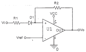
What would be the output of the following circuit, if a positive going unipolar pulse with an amplitude greater than V
ref , is applied at the input?
A. Vo will go high momentarily and return to low
B. Vo will go low momentarily and return to high
C. Vo will go high and remain high
D. Vo will not change its previous state
Select an option to see the answer and solution.
A high gain OpAmp has Rf = 105 Ω & Ri = 103 Ω. The correct statements is:
A. The non-inverting gain & inverting gain are nearly same
B. The inverting gain is very much higher than non-inverting gain
C. The non-inverting gain is very much higher than inverting gain
D. The inverting & non-inverting gains are unrelated
Select an option to see the answer and solution.
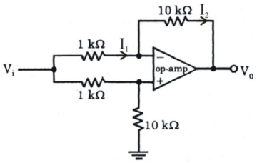
The V
0 of the op-amp circuit shown in the given figure is
Select an option to see the answer and solution.
The main advantage in using three op-amp instrumentation amplifier over a single stage op-amp differential amplifier lies in
A. Higher value of CMRR
B. Lower noise figure
C. Elimination of the need for accurate matching of resistor
D. Simplicity of gain adjustment
Select an option to see the answer and solution.
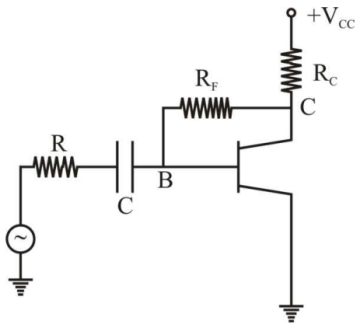
In the circuit shown in the given figure, R
F provides
A. Current series feedback
B. Current shunt feedback
C. Voltage series feedback
D. Voltage shunt feedback
Select an option to see the answer and solution.
An n-channel enhancement mode MOSFET is biased at VGS > VTH and VDS > (VGS - VTH ), where VGS is the gate-to-source voltage. VDS is the drain-to-source voltage and VTH is the threshold voltage. Considering channel length modulation effect be significant, the MOSFET behaves as a
A. Voltage source with zero output impedance
B. Voltage source with non-zero output impedance
C. Current source with finite output impedance
D. Current source with infinite output impedance
Select an option to see the answer and solution.
For an OPAMP, unity gain frequency is 106 if gain is 20, What is the Bandwidth of the op-amp . . . . . . . .
A. 60 kHz
B. 50 kHz
C. 40 kHz
D. 100 kHz
Select an option to see the answer and solution.
The cross-over distortion in class B push-pull amplifier is eliminated by
A. Operating the amplifier as class C
B. Operating the amplifier as class AB
C. Eliminating the output transformer
D. Reducing the biasing of the transistors
Select an option to see the answer and solution.
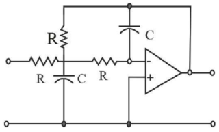
The transfer function of a second order low pass filter shown in Figure is
A. R 2 C 2 s 2 + 3 RCs + 1 1
B. R 2 C 2 s 2 + 3 RCs + 1 RCs
C. R 2 C 2 s 2 + 3 RCs + 1 R 2 C 2 s 2 + 1
D. R 2 C 2 s 2 + 3 RCs + 1 R 2 C 2 s 2
Select an option to see the answer and solution.
The data sheet for a certain JFET ( Junction Field Effect Transistor) indicates that IDSS (drain to source current with gate shorted) = 15 mA and VGS(off) (Cut-off value of gate to source voltage) = -5V. What is the drain current for VGS = -2V?
A. 58.8 mA
B. 29.4 mA
C. 9.6 mA
D. 5.4 mA
Select an option to see the answer and solution.
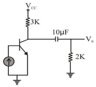
The lower cut-off frequency of the transistor stage in the adjoining figure is
A. 7.95 Hz
B. 13.25 Hz
C. 5.30 Hz
D. 3.18 Hz
Select an option to see the answer and solution.
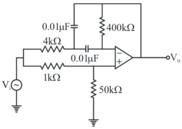
The circuit given in the figure is a
A. Low-pass filter
B. High-pass filter
C. Band-pass filter
D. Notch filter
Select an option to see the answer and solution.
A monostable multivibrator is frequently used:
A. In memory and timing circuit
B. For regeneration of distorted waves
C. In counting circuits
D. For producing triangular waves
Select an option to see the answer and solution.
The phase shift oscillator requires
A. 180° phase shift from RC network
B. 360° phase shift from RC network
C. 0° phase shift from RC network
D. 90° phase shift from RC network
Select an option to see the answer and solution.
The Class-B push-pull amplifier is an efficient two-transistor circuit, in which the two transistors operate in the following way:
A. Both transistors operate in the active region throughout the negative ac cycle
B. Both transistors operate in the active region for more than half-cycle but less than a whole cycle
C. One transistor conducts during the positive half-cycle and the other during the negative half-cycle
D. Full supply voltage appears across each of the transistors
Select an option to see the answer and solution.
The common-mode voltage gain is . . . . . . . .
A. smaller than differential voltage gain
B. equal to differential voltage gain
C. greater than differential voltage gain
D. none of the above
Select an option to see the answer and solution.
Introducing a resistor in the emitter of a common emitter amplifier stabilizes the dc operating point against variation in
A. only the temperature
B. only the β of the transistor
C. both temperature and β
D. none of the above
Select an option to see the answer and solution.
gm of MOSFET is controlled by
A. gate-source voltage
B. drain-source voltage
C. drain current
D. gate current
Select an option to see the answer and solution.
A 741 OP-AMP has an open loop gain 200,000. The output offset voltage is 2 mV. If the input terminals are shorted, the output voltage is
Select an option to see the answer and solution.