Vidyalelo
ECE · all questions

Analog Electronics
practice.

Practice every MCQ with options. Use Show answers when you want the correct option and solution.

377

Questions

7/19

Page

Pick an option on a question to see the right answer and solution.

The voltage divider bias circuit is used in amplifiers quit often because it

Select an option to see the answer and solution.

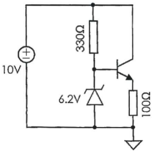
The zener diode shown in following figure is temperature compensated and current gain β of transistor is very high. If current through 100 ohm resistor is 55 mA at 25°C, what is the approximate current through it at 65°C
Analog Electronics mcq question image

Select an option to see the answer and solution.

The output time period of a transistorized monostable multivibrator using base resistance Rb and coupling capacitor Cb for the output transistor is given by

Select an option to see the answer and solution.

In a BJT, the Ic = 30 mA. If β = 100, the base current approximately equals

Select an option to see the answer and solution.

Negative voltage feedback in amplifiers
S1: Improves gain stability
S2: Reduces non linear distortion
S3: Improves frequency response
S4: Increase circuit stability
S5: Increase Input Impedance and decrease output impedance

Select an option to see the answer and solution.

Transformer utilization factor of half wave rectifier is

Select an option to see the answer and solution.

An output signal of a power amplifier has amplitudes of 2.5 V fundamental, 0.25 V second harmonic and 0.1 V third harmonic. The total percentage harmonic distortion of the signal is

Select an option to see the answer and solution.

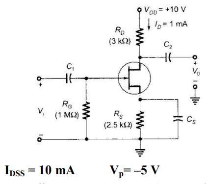
The voltage gain Av =  of the JFET amplifier shown in the figure is
Analog Electronics mcq question image
(Assume C1, C2 and Cs to be very large)

Select an option to see the answer and solution.

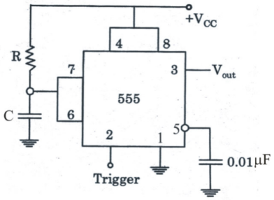
The circuit shown above is:
Analog Electronics mcq question image

Select an option to see the answer and solution.

If the bias current in the IC-741 op-amp is IQ = 19 µA and the internal frequency compensation capacitor C1 = 30 pF, the slew rate of the op-amp will be nearly

Select an option to see the answer and solution.

Which class of amplifier has the lowest collector circuit efficiency

Select an option to see the answer and solution.

Consider the following statements:
Sziklai pair
1. Is also called complementary Darlington
2. Acts like a single p-n-p transistor with a very high current gain
3. Can be used in class B push-pull power amplifier
Which of these statements are correct?

Select an option to see the answer and solution.

In an op-amp, non-inverting terminal is grounded, input is connected to inverting terminal and there is no feedback resistance. The output is

Select an option to see the answer and solution.

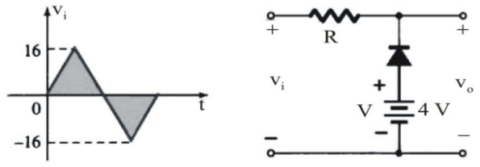
What are the output voltage levels for the given circuit? (Assume Si diode)
Analog Electronics mcq question image

Select an option to see the answer and solution.

A bipolar junction transistor is in saturation region. Given VCC = 10 V, RC = 1 kΩ, hFE = 100 and VCEsat = 0.3 V. What is the collector current in saturation?

Select an option to see the answer and solution.

The first dominant pole encountered in the frequency response of a compensated op-amp is approximately at

Select an option to see the answer and solution.

In the Wien bridge oscillator, the 0° phase-shift is met by using lead-lag network and by using.

Select an option to see the answer and solution.

Among CB, CE and CC configurations of the amplifiers, which is having low voltage gain and high current gain?

Select an option to see the answer and solution.

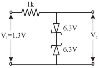
The output voltage (V0) of the circuit shown in the given figure is
Analog Electronics mcq question image

Select an option to see the answer and solution.

An amplifier without feedback has a voltage gain of 50, input resistance of 1 kΩ and output resistance of 2.5 kΩ. The input resistance of the current-shunt negative feedback amplifier using the above amplifier with a feedback factor of 0.2 is

Select an option to see the answer and solution.