The term AB + AC + BC reduces to
A. AB + CA
B. AC + BC
C. AC + B C
D. AB + B C
Select an option to see the answer and solution.
A digital-to-analog converter with a full scale output voltage of 3.5 V has a resolution close to 14 mV. Its bit size is
Select an option to see the answer and solution.
The logic expression y = A + A B
A. y = AB
B. y = A B
C. y = A + B
D. y = A + B
Select an option to see the answer and solution.
What value of x satisfies the equation
( 121 ) 7 = ( x ) 2 ?
(where integer numbers written as subscripts are the base of the corresponding number systems.)
Select an option to see the answer and solution.
A B + AB,
Select an option to see the answer and solution.
The difference between PLA and ROM is
A. PLA is sequential, ROM is combinational
B. PLA is combinational ROM is sequential
C. PLA is economizes on the number of min-term to implement Boolean functions
D. PLA has fixed AND array, ROM has fixes OR array
Select an option to see the answer and solution.
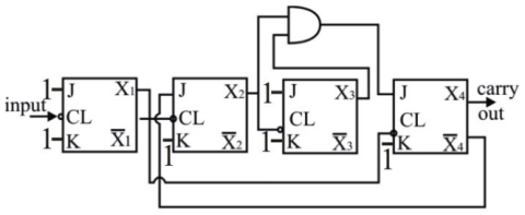
The schematic shown in the figure represents
A. Divide by seven counter
B. Divide by five counter
C. Binary coded decimal counter
D. Divide by twelve counter
Select an option to see the answer and solution.
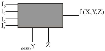
If a 4-to-1 MUX (shown below) realizes a three-variable function f(X, Y, Z) = XY + X
Z . Then which of the following is correct?
A. I0 = X, I1 = 0, I2 = X, I3 = X
B. I0 = 0, I1 = 1, I2 = Y, I3 = X
C. I0 = X, I1 = 1, I2 = 0, I3 = X
D. I0 = X, I1 = 0, I2 = X, I3 = Z
Select an option to see the answer and solution.
Consider the logic circuit with input signal TEST shown in the figure. All gates in the figure shown have identical non-zero delay. The signal TEST which was at logic LOW is switched to logic HIGH and maintained at logic HIGH. The output:
A. Stays LOW throughout
B. Pulses from LOW to High to LOW
C. Stays HIGH throughout
D. Pulses from HIGH to LOW to HIGH
Select an option to see the answer and solution.
An R-S latch is
A. combinational circuit
B. synchronous sequential circuit
C. one bit memory element
D. one clock delay element
Select an option to see the answer and solution.
The binary number 101 represents:
A. -3 in two's complement system
B. 7 in sign magnitude system
C. -5 in two's complement system
D. -2 in sign magnitude system
Select an option to see the answer and solution.
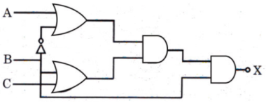
The output X of the logic circuit shown in the figure is
Select an option to see the answer and solution.
A digital frequency converter can be converted to DVM by addition of a suitable
A. VCO
B. D/A converter
C. power amplifier
D. Op-Amp
Select an option to see the answer and solution.
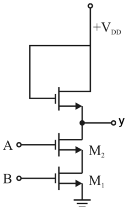
The circuit shown in figure is
A. OR gate
B. NOR gate
C. NAND gate
D. AND gate
Select an option to see the answer and solution.
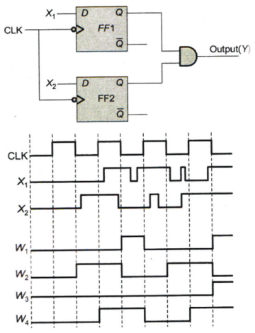
In the circuit shown, choose the correct timing diagram of the output (Y) from the given waveforms W
1 , W
2 , W
3 and W
4 .
Select an option to see the answer and solution.
Which of the following statements about the K-maps is INCORRECT?
A. In K-maps, don't care terms are used only if they help in reducing the expression. Otherwise, they need not be considered
B. A two-variable K-map expression can have 4 possible combinations of the input variables
C. The binary number designations of the rows and columns of the K-map are in Gray code
D. The five-variable map may contain 2-squares, 4-squares, 8-squares, or other combinations involving four blocks of K-map having 16 squares each
Select an option to see the answer and solution.
If (432)5 = (x)7 , then the value of x is
Select an option to see the answer and solution.
Given (125)R = (203)5 . The value of radix R will be
Select an option to see the answer and solution.
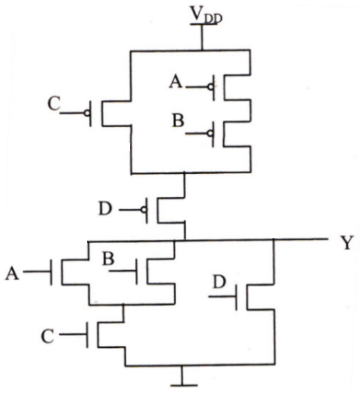
Find Y
A. ( A + B ) C + D
B. ( A + B ) C + D
C. [ ( A . B ) + C ] . D
D. [ ( A . B ) + C ] . D
Select an option to see the answer and solution.
A 4-bit presetable UP counter has preset input 0101. The preset operation takes place as soon as the counter reaches 1111. The modulus of the counter is
Select an option to see the answer and solution.