A 12-bit ADC is employed to convert an analog voltage of zero to 10 volts. The resolution of the ADC is
A. 2.44 mV
B. 24.4 mV
C. 83.3 mV
D. 1.2 V
Select an option to see the answer and solution.
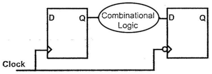
What is the maximum clock frequency at which following circuit can be operated without timing violations? Assume that the combinational logic delay is 10 ns and the clock duty cycle varies form 40% to 60%
A. 100 MHz
B. 50 MHz
C. 40 MHz
D. 25 MHz
Select an option to see the answer and solution.
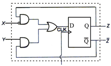
A sequential circuit using D Flip-Flop and logic gates is shown in the figure, where X and Y are the inputs and Z is the output. The circuit is
A. S-R Flip-Flop with inputs X = R and Y = S
B. S-R Flip-Flop with inputs X = S and Y = R
C. J-K Flip-Flop with inputs X = J and Y = K
D. J-K Flip-Flop with inputs X = K and Y = J
Select an option to see the answer and solution.
The output of the 74 series gate of TTL gates is taken from a BJT in
A. totem pole and common collector configuration
B. either totem pole or open collector configuration
C. common base configuration
D. common collector configuration
Select an option to see the answer and solution.
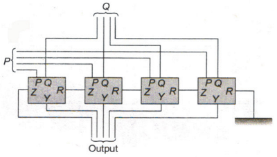
The circuit shown in the figure has 4 boxes each described by inputs P, Q, R and outputs Y, Z with
Y = P ⊕ Q ⊕ R, Z = RQ + P R + Q P
The circuit acts as a
A. 4 bit adder giving P + Q
B. 4 bit subtractor giving P - Q
C. 4 bit subtractor giving Q - P
D. 4 bit adder giving P + Q + R
Select an option to see the answer and solution.
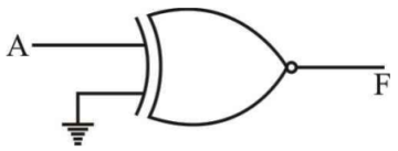
For the gate in the given figure the output will be . . . . . . . .
Select an option to see the answer and solution.
The 54/74164 chip is as 8-bit serial-input-parallel-output shift register. The clock is 1 MHz. The time needed to shift an 8-bit binary number into the chip is
A. 1 µs
B. 2 µs
C. 8 µs
D. 16 µs
Select an option to see the answer and solution.
For the code X1 = (000, 111) how many errors can be successfully detected?
A. upto two
B. upto three
C. upto seven
D. upto four
Select an option to see the answer and solution.
IC 74 HC00 series belong to,
A. High Speed TTL IC
B. High Speed CMOS IC
C. Low power Schottkey TTL
D. MSI family
Select an option to see the answer and solution.
In S-R latch, when the SET input is made high, output Q becomes:
A. 0
B. application not allowed
C. 1
D. no change
Select an option to see the answer and solution.
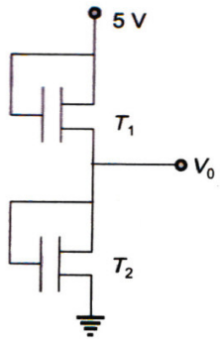
Both transistors T
1 and T
2 shown in the figure, have a threshold voltage of 1 Volts. The device parameters K
1 and K
2 of T
1 and T
2 are respectively, 36 µA/V
2 and 9 µA/V
2 . The output voltage V
0 is
Select an option to see the answer and solution.
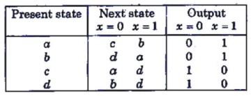
In the following state table, the equivalent states are
A. (a, d)(b, c)
B. (a, c)(b, d)
C. (a, b)(c, d)
D. (a, c)
Select an option to see the answer and solution.
The expression for the truth table given below in POS form is given by:
A B
C
F
0 0
0
1
0 0
1
0
0 1
0
1
0 1
1
1
1 0
0
1
1 0
1
1
1 1
0
1
1 1
1
0
A. AB'C + ABC'
B. (A + B + C')(A' + B' + C')
C. A'B'C + ABC
D. (A + B' + C')(A' + B' + C')
Select an option to see the answer and solution.
Consider the following statements regarding configuration of TTL devices:
A. 1 and 2 are correct
B. 1, 3 and 4 are correct
C. 2 and 3 are correct
D. 2, 3 and 4 are correct
Select an option to see the answer and solution.
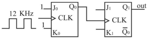
An input frequency of 12 KHz is applied to the J-K flip-flops arrangement shown in the given figure. The resulting output frequency will be
A. 24 KHz
B. 12 KHz
C. 6 KHz
D. 3 KHz
Select an option to see the answer and solution.
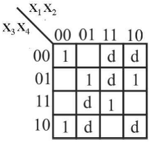
Consider the Karnaugh map given below : The function represented by this map can be simplified to the minimal form as
A. x 1 x 2 x 4 + x 2 x 4 + x 1 x 3
B. x 1 x 2 x 4 + x 2 x 4 + x 1 x 2 x 3 x 4
C. x 2 x 4 + x 2 x 4 + x 1 x 3
D. x 1 x 2 x 4 + x 1 x 2 x 3 x 4 + x 1 x 2
Select an option to see the answer and solution.
Which one of the following Boolean expressions is NOT correct?
A. x + y = x y
B. x + y = x y
C. x + y = x + y
D. x + y = xy
Select an option to see the answer and solution.
The number of digit 1 present in the binary representation of 3 × 512 + 5 × 64 + 7 × 8 + 3 is:
Select an option to see the answer and solution.
The fastest ADC among the following is
A. Successive approximation type
B. Dual slope type
C. Sigma-Delta ADC
D. Flash converter
Select an option to see the answer and solution.
What will be the simplified Boolean function of the given equation? F(a, b, c) = Σ(0, 2, 4, 5, 6)
A. ac' + b
B. c' + ab'
C. a + b + c
D. a'b + c
Select an option to see the answer and solution.