Number of electron-hole pairs generated per incident photon is called . . . . . . . .
A. Power efficiency
B. Luminescence efficiency
C. Optical efficiency
D. Frequency response
E. Quantum efficiency
Select an option to see the answer and solution.
The best electronic device for fast switching is
A. BJT
B. triac
C. JFET
D. MOSFET
Select an option to see the answer and solution.
In an extrinsic semiconductor the conductivity significantly depends upon:
A. Majority charge carriers generated due to impurity doping
B. Minority charge carriers generated due to thermal agitation
C. Majority charge carriers generated due to thermal agitation
D. Minority charge carriers generated due to impurity doping
Select an option to see the answer and solution.
Consider the following statements regarding the formation of P-N junctions:
A. 1 and 3
B. 2 and 3
C. 1 and 4
D. 2 and 4
Select an option to see the answer and solution.
The doping concentration on the p-side and n-side of a silicon diode are 1 × 1016 cm-3 , and 1 × 1017 cm-3 respectively. A forward bias of 0.3 V is applied to the diode. At T = 300 K, the intrinsic carrier concentration of silicon ni = 1.5 × 1010 cm-3 and q kT
A. 2.3 × 109 cm-3
B. 1 × 1016 cm-3
C. 1 × 1017 cm-3
D. 2.25 × 106 cm-3
Select an option to see the answer and solution.
Which of the following is true?
A. A silicon wafer heavily doped with boron is a p+ substrate
B. A silicon wafer lightly doped with boron is a p+ substrate
C. A silicon wafer heavily doped with arsenic is a p+ substrate
D. A silicon wafer lightly doped with arsenic is a p+ substrate
Select an option to see the answer and solution.
If the current in a diode is 10 mA at forward bias voltage of 0.1 V, static resistance is
A. 10 Ω
B. 100 Ω
C. 1 kΩ
D. 0.01 Ω
Select an option to see the answer and solution.
The number of LED display indicators in logic probes are
Select an option to see the answer and solution.
Medium doping in Silicon and Germanium corresponds to impurity of the order of
A. 1 part in 106
B. 1 part in 105
C. 1 part in 104
D. 1 part in 108
Select an option to see the answer and solution.
List-I is four different semiconductor devices. Match each device in
List-I with its characteristic property in
List-II .
List-I List-II
a. BJT
1. Population inversion
b. MOS capacitor
2. Pinch-off voltage
c. LASER diode
3. Early effect
d. JFFT
4. Flat-band voltage
A. a-2, b-1, c-4, d-2
B. a-1, b-4, c-3, d-2
C. a-3, b-4, c-1, d-2
D. a-3, b-2, c-1, d-4
Select an option to see the answer and solution.
What is one of the primary advantages of FET compared to BJT?
A. Low input impedance
B. Low output impedance
C. High input impedance
D. High output impedance
E. Low value of current
Select an option to see the answer and solution.
Why is silicon dioxide (SiO2 ) layer used in ICs?
A. To protect the surface of the chip from external contaminants and to allow for selective formation of the n and p regions by diffusion
B. because it facilitates the penetration of the desired impurity by diffusion
C. To control the concentration of the diffused impurities by diffusion
D. Because of its high heat conduction
Select an option to see the answer and solution.
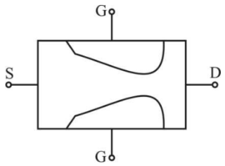
In a biased JFET, the shape of the channel is as shown in the given figure. because
A. it is the property of the material used
B. the drain end is more reverse biased than source end
C. the drain end is more forward biased than source end
D. the impurity profile varies with the distance from source
Select an option to see the answer and solution.
Practically, in order to create an electron-hole pair in a P-N junction diode, the energy of the incident photon should be
A. Less than the band gap
B. Equal to the band gap
C. Greater than the band gap
D. None of the above
Select an option to see the answer and solution.
In order to generate electron-hole pairs, the maximum wavelength of radiation for Silicon (Band gap = 1.1 eV) is
A. 1.88 µm
B. 1.68 µm
C. 1.13 µm
D. 1.54 µm
Select an option to see the answer and solution.
The diffusion potential across P-N junction
A. Decreases with increasing doping concentration
B. Increases with decreasing band gap
C. Does not depend on doping concentrations
D. Increases with increase in doping concentration
Select an option to see the answer and solution.
The quantum efficiency η for the photo detector isph = Average photocurrente = Average incident optical power
A. P 0 I ph
B. P 0 /(hc/ λ ) I ph /e
C. I ph P 0
D. I ph /e P 0 /(hc/ λ )
Select an option to see the answer and solution.
Which statement is correct for Schottky diode?
A. Current Voltage characteristics is totally different than that of a p-n junction diode
B. The current is controlled by the diffusion of minority carriers
C. The current results from the flow of minority carriers
D. The storage time ts is almost zero
Select an option to see the answer and solution.
Assuming that the electron mobility in intrinsic silicon is 1500 cm2 /V-Sec at room temperature (T = 300 K and the corresponding 'volt equivalent of temperature' VT = 25.9 mV, what is the approximate value of the electron diffusion constant?
A. 40 cm2 /s
B. 4 cm2 /s
C. 400 cm2 /s
D. 4000 cm2 /s
Select an option to see the answer and solution.
In a forward-biased p-n diode with NA >> ND , the product of dynamic diode resistance and diffusion capacitance CD equals:
Select an option to see the answer and solution.